

MicroLED: Emerging as a Next Generation Display Technology
MicroLED is emerging as next generation display technology because of its potential to be a thinner, brighter, lighter, and low power display. It combines the best features of LCD and OLED. It is considered by some to be the fourth generation flat panel display technology after, Plasma, LCD and OLED.
It is not yet commercialized or in mass production. But working prototypes are showing up this year, as seen at CES 2019. Many companies are also working within the MicroLED display supply chain to resolve manufacturing issues, improve yields and reduce costs to enable volume productions for consumer products. There are still many challenges to be solved. Can MicroLED compete with LCD and OLED?
Simple structure but complex manufacturing process
MicroLED is a self-emitting display which consist of arrays of microscopic LEDs each forming a pixel. It is simple in structure compared to OLED and LCD but has a complex manufacturing process. Display integration of MicroLED can be generally of two types.
One is heterogeneous integration, where MicroLED arrays use pick and place process, and chips are transferred from an epiwafer or carriers to the display backplane.
The other one is monolithic integration where process involves MicroLED arrays and backplane hybridization.
According to industry estimates, more than 130 companies are working in the MicroLED display supply chain including Apple (LuxVue), Oculus (InfiniLED) Samsung, LG Display, AUO, Sony, eLux (integrated with Foxconn group), Aledia (Intel), Lumens, Lumiode, Jade Bird, Mikro Mesa, Play Nitride, Plessey, Glo (Google), X-celeprint, Rohinni, Sony, Visionox and others. MicroLED display has many advantages such as high brightness, ultra low power consumption, fast response time, very high contrast rate, wide color gamut, long lifetime, environmental stability, high resolution, the option of flexible backplanes and integration of sensors in the display. Its main challenges are manufacturing complexity and yield issues.
On the way to resolve manufacturing issues and improve yield
Manufacturing and yield issues can become an issue in epitaxy, chip, and mass transfer, bonding, driving technology, backplane, inspection and repair. The industry is working towards resolving each of these issues. MicroLED chips need wavelength uniformity and thickness uniformity for display applications. Solutions from MOCVD suppliers such as Aixtron, Veeco and others are helping to resolve such issues. For example Veeco is collaborating with Allos (provider of GaN epiwafer technology) to achieve extremely good emission wavelength uniformity, which eliminates the need, to test and sort individual MicroLED chips.
Aixtron is collaborating with PlayNitride for the manufacturing of GaN-based MicroLED. The Aixtron MOCVD solution is enabling high volume manufacturing of products with high-level wavelength uniformity. The system allows for lower defects and particle level, due to in-situ cleaning technology and a cassette-to-cassette handler, which enables higher yield. IP activities have seen strong growth in the last few years – mass transfer technology and chip manufacturing process technology are among the top topics for patents. News sources have reported that PlayNitride’s MicroLED chips were transferred to a glass backplane using Samsung’s mass transfer technology to create the 75-inch MicroLED TV that was shown at CES this year.

MicroLED companies also need to use mass testing and repair methods to reduce the cost and time of assembly. Companies such as Toray are working on equipment for MicroLED wafer inspection, repair and transfer. Laser repair equipment can remove defective MicroLEDs and then selectively transfer good MicroLEDs to complete the repair process.
Producing an RGB (Red Green Blue) MicroLED also has many challenges, as each color MicroLED chip is different. Different colors of LED need slightly different voltage and drive currents. Mechanical placement of these three-color chips is very difficult. Color conversion by Quantum dots or by phosphor provides another alternative. Using single-color (blue) MicroLED chips and color converting them with Quantum dot layers can help in the manufacturing process. Nanosys has demonstrated a photo lithography-patterned cadmium free color conversion layer for MicroLED.
MicroLED display prototypes coming to market
At the DisplayWeek 2018 conference last year, we saw some actual prototypes of MicroLEDs including from companies such as
- Hong Kong Jade Bird Display (active MicroLED with 5000PPI, 1million cd/m² brightness),
- Play Nitride (transparent RGB MicroLED),
- glo and Jasper Display (who together created a high brightness 10 micron silicon backplane for watch, HUD, AR and other applications) as well as
- AUO (8-inch full color, 169PPI, LTPS backplane MicroLED).
- Samsung showcased its 75-inch true MicroLED TV this year at CES.
- Plessey, PlayNitride, Lumiode, and Lumen showed new MicroLED display prototypes at CES.
- Plessey was awarded as a CES 2019 Innovation Awards Honoree for its GaN-on-silicon monolithic MicroLED that can be used for AR/VR and HUDs applications. It has been working with Vuzix to develop MicroLED-based AR smartglasses.
- Glo showed a prototype of a 1.5-inch 264ppi RGB wearable display with LTPS backplane and a 0.7”1000ppi RGB display for AR/HUD on CMOS backplane.
As I have written in a previous Display Daily article, glo uses existing commercial LTPS glass backplanes and existing volume LED-manufacturing equipment and capacity. With highly selective direct wafer transfer capability glo technology can scale to all size and resolutions (micro display, mobile display and large display) on either a CMOS or LTPS backplane. According to the company, leveraging existing LED and LCD industry infrastructure glo’s micro LED display can be cost competitive with high end OLED and expected to have even more competitive cost curve going forward.
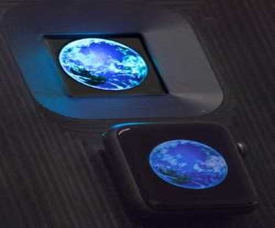
glo MicroLED watch display prototype

Plessey native Green MicroLED
Opportunities for wide range of applications
MicroLED’s ability to create high brightness and high resolution images with low power consumption gives it certain advantages over current display technology in applications such as wearable (smart watch and fitness trackers) and AR/VR. MicroLED-based display devices for wearable and AR/VR are expected to be available in the 2019-2020 timeframe.
Smartwatch displays are small in size but they need high resolution and higher brightness for outdoor use with longer battery life. MicroLED will be able to meet these requirements and it is expected to exceed OLED in terms of brightness and power efficiency. Apple is reportedly working on MicroLED after acquiring LuxVue. Oculus has acquired InfiniLED to incorporate MicroLED into VR headsets for high resolutions and immersive experience.
Companies are initially targeting wearable, AR/VR, digital signage, public display and automotive (HUD) applications. High-speed transfer, assembly technologies, yield and defect management are still under development before large volume commercialization in consumer products such as smartphones or TV.
Implications for the display industry
LCD and OLED technology are moving targets, both still improving in performance and reducing their costs. Can MicroLED potentially match the price and performance of LCD and OLED? In theory, it can. But as history has shown, theoretical potential takes years to be realized and sometimes never gets there. MicroLED with its exceptional potential faces many challenges (manufacturing yield issues and high cost) and industry suppliers are all working to bring MicroLED potential to reality, but it will take time. Success will depend on its ability to scale up for volume production with competitive price performance – SD
Source : www.displaydaily.com
